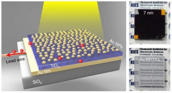
Scientists have developed a photoelectrode that can harvest 85 percent of visible light in a 30 nanometers-thin semiconductor layer between gold layers, converting light energy 11 times more efficiently than previous methods.
In the pursuit of realizing a sustainable society, there is an ever-increasing demand to develop revolutionary solar cells or artificial photosynthesis systems that utilize visible light energy from the sun while using as few materials as possible.
The research team, led by Professor Hiroaki Misawa of the Research Institute for Electronic Science at Hokkaido University, has been aiming to develop a photoelectrode that can harvest visible light across a wide spectral range by using gold nanoparticles loaded on a semiconductor. But merely applying a layer of gold nanoparticles did not lead to a sufficient amount of light absorption, because they took in light with only a narrow spectral range.
In the study published in Nature Nanotechnology, the research team sandwiched a semiconductor, a 30-nanometer titanium dioxide thin-film, between a 100-nanometer gold film and gold nanoparticles to enhance light absorption. When the system is irradiated by light from the gold nanoparticle side, the gold film worked as a mirror, trapping the light in a cavity between two gold layers and helping the nanoparticles absorb more light.
Read more at Hokkaido University
Image: Left: The newly developed photoelectrode, a sandwich of semiconductor layer (TiO2) between gold film (Au film) and gold nanoparticles (Au NPs). The gold nanoparticles were partially inlaid onto the surface of the titanium dioxide thin-film to enhance light absorption. Right: The photoelectrode (Au-NP/TiO2/Au-film) with 7nm of inlaid depth traps light making it nontransparent (top). An Au-NP/TiO2 structure without the Au film are shown for comparison (bottom). (Credit: Misawa H. et al., Nature Nanotechnology, July 30, 2018)


